21
LTC3445
3445fa
As an example, consider the LTC3445 in dropout at an
input voltage of 2.7V, an ambient temperature of 70癈, a
buck load current of 600mA, LDO1 set to 1.3V with a load
of 25mA, LDO2 set to 1.1V with a load of 15mA, and the
PowerPath regulator at 2.5V with a load of 6礎. From the
typical performance graph of switch resistance, the R
DS(ON)
of the P-channel switch at 70癈 is approximately 0.52&.
Therefore, power dissipated by the part is:
P
D(BUCK)
= I
LOAD
2
" R
DS(ON)
= 180mW
P
D(LDO1)
= (2.7 1.3)V " 0.025A = 35mW
P
D(LDO2)
= (2.7 1.1)V " 0.015A = 24mW
P
D(PowerPath)
= (2.7 2.5)V " 6礎 = 1.2礧
P
D(TOTAL)
= 0.239W
For the QFN24 package, the ?/DIV>
JA
is 37癈/W. Thus, the
junction temperature of the regulator is:
T
J
= 70癈 + (0.239)(37) = 78.8癈
which is well below the maximum junction temperature of
125癈. Note that at higher supply voltages, the junction
temperature is lower due to reduced switch resistance
(R
DS(ON)
).
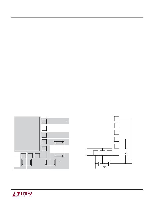
PC BOARD LAYOUT CHECKLIST
When laying out the printed circuit board, the following
checklist should be used to ensure proper operation of the
LTC3445. These items are also illustrated graphically in
Figures 9 and 10. Check the following in your layout:
1. The power traces, consisting of the GND trace, the SW
trace, the V
CC1
trace and the V
CC2
trace should be kept
short, direct and wide.
2. Does the FB pin connect directly to the output voltage
reference? Ensure that there is no load current running
from the reference voltage and the FB pin.
3. Does the (+) plate of C
IN1
connect to V
CC1
as closely as
possible? This capacitor provides the AC current to the
internal power MOSFETs.
4. Keep the switching node, SW, away from the sensitive
FB node.
5. Keep the () plates of C
IN
and C
OUT
as close as possible.
APPLICATIO S I FOR ATIO
U
U
U
Figure 9
Figure 10
V
CC1
10
V
CC1
GND
OUT
3445 F09
SW
RUN
FB
GND
25
NC
12
GND
11
NC
13
SW
14
RUN
15
NC
16
VIA TO
OUT
VIA TO
FB
FB
17
C
IN
C
OUT
L1
V
CC1
10
3445 f10
GND
25
L1
V
OUT
BOLD LINES INDICATE HIGH CURRENT PATH
V
CC1
C
IN
NC
12
GND
11
NC
13
SW
14
RUN
15
NC
16
FB
17
C
OUT
发布紧急采购,3分钟左右您将得到回复。
相关PDF资料
LTC3446IDE#PBF
IC REG TRPL BCK/LINEAR 14-DFN
LTC3537EUD#TRPBF
IC REG DL BST/LINEAR SYNC 16-QFN
LTC3541EDD#TRPBF
IC REG DL BCK/LINEAR SYNC 10-DFN
LTC3670EDDB#TRPBF
IC REG TRPL BCK/LINEAR 12DFN
LTC3672BEDC-1#TRPBF
IC REG TRPL BCK/LINEAR 8-DFN
LTC3700EMS#TRPBF
IC REG DL BUCK/LINEAR 10MSOP
LTC4151HMS#TRPBF
IC PWR MONITOR MS 80V SD 10MSOP
LTC4210-2CS6#TRM
IC CONTROLLER HOT SWAP TSOT23-6
相关代理商/技术参数
LTC3446
制造商:LINER 制造商全称:Linear Technology 功能描述:Monolithic Buck Regulator with Dual VLDO Regulators
LTC3446EDE
制造商:LINER 制造商全称:Linear Technology 功能描述:Monolithic Buck Regulator with Dual VLDO Regulators
LTC3446EDE#PBF
功能描述:IC REG TRPL BCK/LINEAR 14-DFN RoHS:是 类别:集成电路 (IC) >> PMIC - 稳压器 - 线性 + 切换式 系列:- 标准包装:2,500 系列:- 拓扑:降压(降压)同步(3),线性(LDO)(2) 功能:任何功能 输出数:5 频率 - 开关:300kHz 电压/电流 - 输出 1:控制器 电压/电流 - 输出 2:控制器 电压/电流 - 输出 3:控制器 带 LED 驱动器:无 带监控器:无 带序列发生器:是 电源电压:5.6 V ~ 24 V 工作温度:-40°C ~ 85°C 安装类型:* 封装/外壳:* 供应商设备封装:* 包装:*
LTC3446EDE#TRPBF
功能描述:IC REG TRPL BCK/LINEAR 14-DFN RoHS:是 类别:集成电路 (IC) >> PMIC - 稳压器 - 线性 + 切换式 系列:- 标准包装:2,500 系列:- 拓扑:降压(降压)同步(3),线性(LDO)(2) 功能:任何功能 输出数:5 频率 - 开关:300kHz 电压/电流 - 输出 1:控制器 电压/电流 - 输出 2:控制器 电压/电流 - 输出 3:控制器 带 LED 驱动器:无 带监控器:无 带序列发生器:是 电源电压:5.6 V ~ 24 V 工作温度:-40°C ~ 85°C 安装类型:* 封装/外壳:* 供应商设备封装:* 包装:*
LTC3446EDE-PBF
制造商:LINER 制造商全称:Linear Technology 功能描述:Monolithic Buck Regulator with Dual VLDO Regulators
LTC3446EDE-TRPBF
制造商:LINER 制造商全称:Linear Technology 功能描述:Monolithic Buck Regulator with Dual VLDO Regulators
LTC3446IDE
制造商:LINER 制造商全称:Linear Technology 功能描述:Monolithic Buck Regulator with Dual VLDO Regulators
LTC3446IDE#PBF
功能描述:IC REG TRPL BCK/LINEAR 14-DFN RoHS:是 类别:集成电路 (IC) >> PMIC - 稳压器 - 线性 + 切换式 系列:- 标准包装:2,500 系列:- 拓扑:降压(降压)同步(3),线性(LDO)(2) 功能:任何功能 输出数:5 频率 - 开关:300kHz 电压/电流 - 输出 1:控制器 电压/电流 - 输出 2:控制器 电压/电流 - 输出 3:控制器 带 LED 驱动器:无 带监控器:无 带序列发生器:是 电源电压:5.6 V ~ 24 V 工作温度:-40°C ~ 85°C 安装类型:* 封装/外壳:* 供应商设备封装:* 包装:*